Our Services
Precision thin film metrology and semiconductor R&D tailored for you.
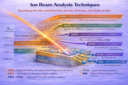
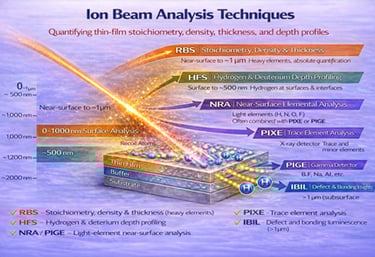


Metrology
Accurate thin film measurements that support your material innovations.
R&D
Collaborative semiconductor research driving your next breakthroughs.
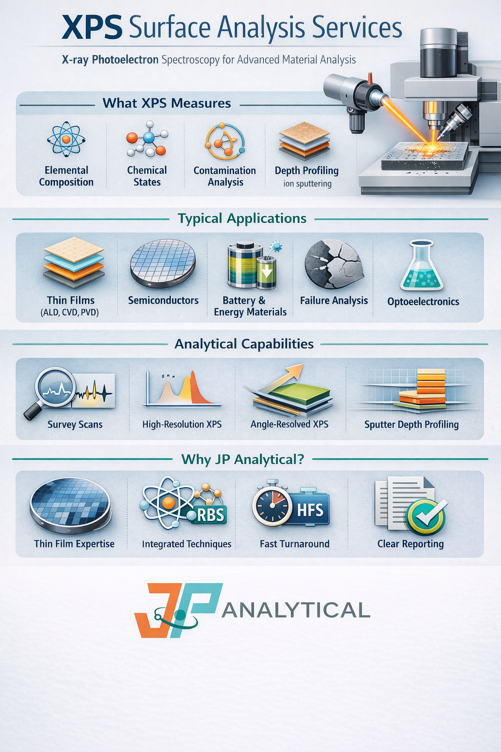
Thin Films
Precision measurements for advanced material layers.

Semiconductor R&D
Supporting semiconductor innovation with detailed metrology and tailored research solutions that drive your projects forward.
Custom Solutions
Developing bespoke analytical tools and methods to meet the unique challenges of your material science projects.
Feedback
What our clients say about us
JP Analytical’s precision and attention to detail helped us improve our thin film processes significantly.
Dr. Lee
Austin TX
Their R&D insights gave our team the edge we needed to push our semiconductor projects forward.
Ms. Chen
San Jose