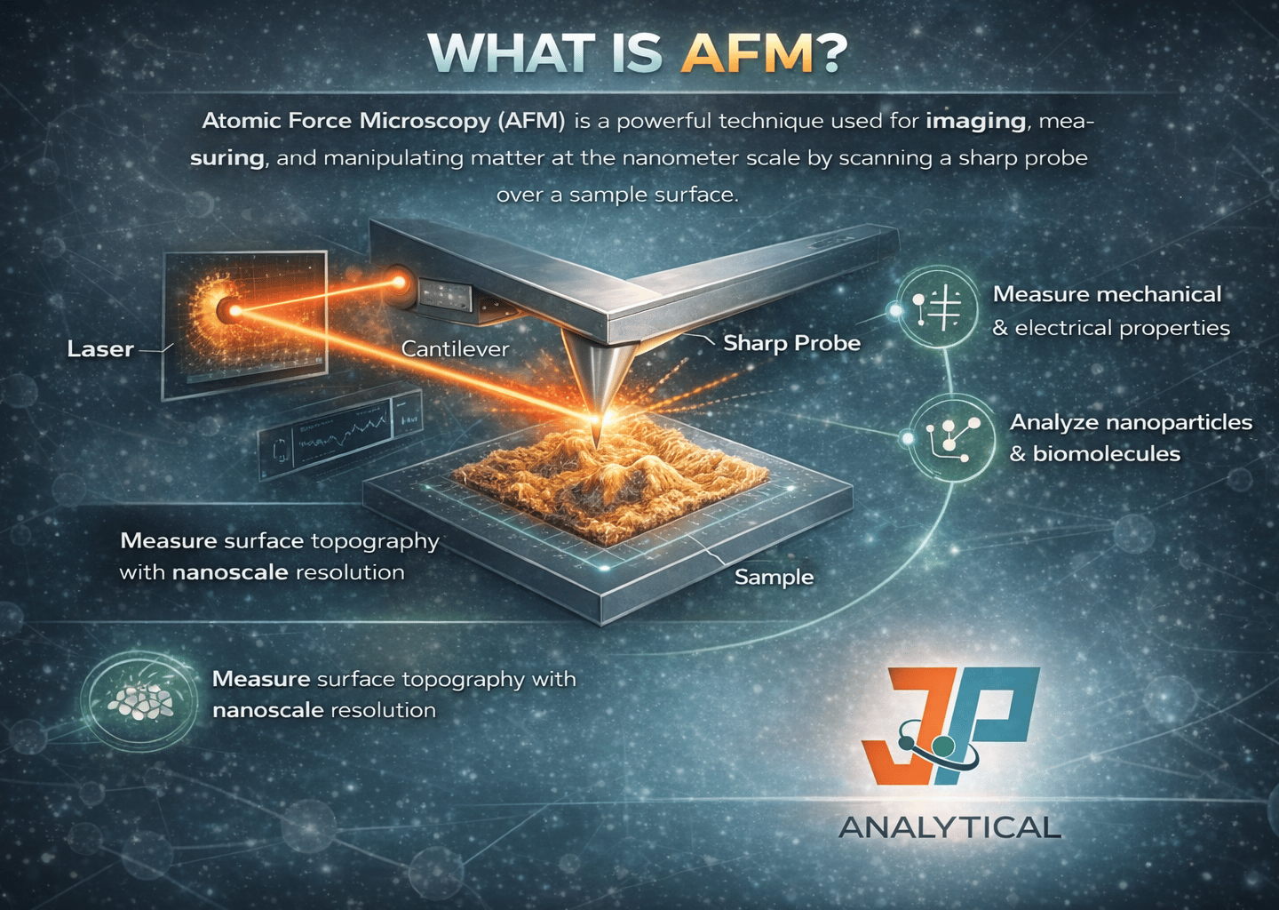
Atomic Force Microscopy (AFM)
Atomic Force Microscopy (AFM) is a high-resolution surface characterization technique that maps nanoscale topography by scanning a sharp probe across the sample surface. At JP Analytical, AFM is used to measure surface roughness, morphology, and mechanical or electrical properties with exceptional spatial precision, providing critical insight into thin-film quality and interface behavior.
AFM complements structural and compositional techniques by delivering real-space surface information, making it especially valuable for advanced semiconductor materials, ALD/CVD/PVD thin films, and defect or process optimization studies where nanoscale surface control directly impacts performance
JP Analytical provides Atomic Force Microscopy (AFM) as part of our advanced metrology services, delivering high-resolution surface characterization at the nanoscale. Our AFM capability complements structural and compositional techniques by providing real-space surface insight, supporting semiconductor and advanced materials development where nanoscale surface control, interface quality, and process optimization directly influence device reliability and yield.